Lattice LC4064V-75TN48C: A Comprehensive Technical Overview of the CPLD
The Lattice LC4064V-75TN48C represents a classic and enduring architecture within the realm of Complex Programmable Logic Devices (CPLDs). Designed for high-performance, low-power, and cost-sensitive applications, this device continues to be a reliable workhorse for countless digital designs, from glue logic and bus interfacing to state machine control and power management sequencing.
Architectural Foundation: The Macrocell Array
At the heart of the LC4064V lies a deterministic, predictable architecture based on a Programmable Interconnect Matrix (PIM) that links multiple Function Blocks. This is a hallmark of traditional CPLD design. The device contains 64 macrocells, organized into four Function Blocks of 16 macrocells each. Each macrocell can be configured for registered or combinatorial logic operations, providing a flexible foundation for implementing a wide variety of logic functions. This array-based structure guarantees fixed timing characteristics, a critical advantage over FPGAs for control-oriented applications where signal path delay must be consistent and predictable.
Performance and Speed Grade
The "-75" suffix in its part number denotes its 5.0ns maximum pin-to-pin propagation delay, making it a member of the high-speed grade within the ispMACH 4000V family. This performance level allows the device to operate at system frequencies well above 100 MHz, ensuring it can handle demanding interface standards and fast state transitions. The speed is specified under worst-case commercial conditions (Vcc = 3.3V, TJ = 70°C), providing a reliable metric for designers.
Power Efficiency and Voltage Operation
A key feature of the 4000V family is its low-power 3.3V core voltage operation. This makes the LC4064V exceptionally suitable for modern, power-conscious electronic systems. The device utilizes an advanced ispMACH process technology that optimizes power consumption without sacrificing performance. Furthermore, it supports 5V tolerant I/Os, allowing it to seamlessly interface with legacy 5V logic devices, which is a significant benefit in mixed-voltage systems and design upgrades.
Package and I/O Capabilities
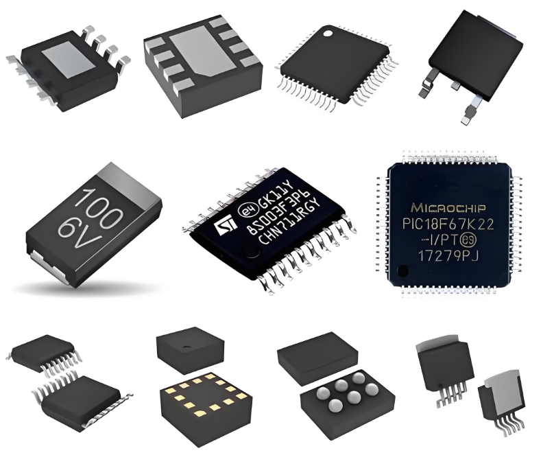
The "TN48C" identifier specifies a 48-pin Thin Plastic Quad Flat Pack (TQFP) package. This compact, surface-mount package is ideal for space-constrained PCB designs. The device offers up to 39 user-defined I/O pins, each of which can be individually configured to comply with various I/O standards. These pins feature programmable bus maintenance and pull-up resistors, enhancing system integration and simplifying board design.

In-System Programmability (ISP)
A defining characteristic of this CPLD is its robust In-System Programmability via the IEEE 1149.1 (JTAG) interface. This allows for rapid design iterations and firmware updates after the device has been soldered onto a printed circuit board. This feature drastically reduces development time, simplifies production flows, and enables field upgrades, extending the product's lifecycle.
Design and Development Support
Designing with the LC4064V is supported by Lattice's ispLEVER classic design software suite. This environment provides a complete set of tools for design entry (schematic or HDL), synthesis, functional simulation, and fitting. The software generates a JEDEC file that is used to program the device, streamlining the path from concept to programmed silicon.
ICGOODFIND: The Lattice LC4064V-75TN48C stands as a testament to the enduring value of the CPLD. It offers a perfect blend of predictable timing, high performance, low power consumption, and 5V I/O tolerance. Its deterministic nature makes it an ideal solution for "connect and control" applications where FPGAs might be overkill. For designers needing reliable glue logic, interface bridging, or simple state machine control in a compact, low-power package, the LC4064V remains a highly compelling and cost-effective choice.
Keywords:
1. CPLD (Complex Programmable Logic Device)
2. Macrocell
3. In-System Programmability (ISP)
4. 5V Tolerant I/O
5. Deterministic Timing
